Xmega DFU Bootloader – Changing the Sensing Pin

The DFU bootloaders that Atmel supplies, as Intel HEX files, for its Xmegas have pre-determined pins used to sense whether or not to skip the bootloader and start the application, or to register the device to the host PC via USB. These are slightly hidden on the Atmel website and the source code requires IAR to compile it (and an easy port to AVR-GCC is thought to be impossible on size grounds). A number of threads on AVRFreaks have discussed this matter, including: “Building bootloader for ATXMega16A4U from avr1916.zip” and “Where’s the DFU bootloader?“. I didn’t fancy installing IAR, but was intrigued by comments about dis-assembling the HEX files and tweaking bytes. The process was not explained, but in spite of starting off totally “in the dark”, an evening of fumbling and fiddling got me through to a result that worked. This post explains the process, in case anyone else wants to do the same. It is also my notes-to-self for when I forget!

Background

The Atmel application note AVR1916 has essential background info and the associated zip file contains the Intel HEX files for different xmega chips. The zip file also contains source code but: a) this needs IAR (see intro); b) it is deeply hard to follow!

Atmel AVR1916: USB DFU Boot Loader for Atmel XMEGA: pdf zip

The zip file is not so easy to find by google/bing; you pretty much have to go to the Atmel site, find the xmega section, go to documents, and select “application notes” from the drop-down.

Tools

There are probably lots of options, but I used:

  • avr-objdump, which is part of the avr-gcc toolchain. I used a recent toolchain download from the Atmel site. If you use Atmel Studio, look in {install directory}\Atmel Toolchain\AVR8 GCC\Native\3.4.1061\avr8-gnu-toolchain\bin.
  • Tiny Hexer by Markus Stephany. This is available from numerous places on the web, although not from the author’s original site mirkes.de .

Procedure

In what follows, I am dealing with an ATxmega32A4U. The method should translate to other chips very easily. I am ONLY concerned with changing which pin is sensed on a hardware reset to determine whether to start the application or wait for USB communication of a new application.

From a command window, execute:

avr-objdump -m avr -D file.hex >> disassembly.txt

That looks somewhat daunting to a non-assembler hobbyist person like me but it turns out not to be quite as bad as all that. The key thing to note is that we’re looking for references to a single I/O pin. Which pin it is may be found in AVR1916.

Default pin configuration table from AVR1916.
Default boot-sensing pin configuration table from AVR1916.

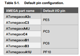
So, for my target it is Port C, pin 3. Consulting the xmega manual…

Base IO memory map addresses for the GPIO ports.
IO port memory map offsets (apply to all ports, simply add to the base address for the port to get the address of the appropriate register)

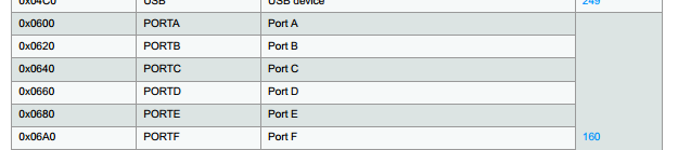
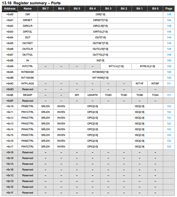
So, setting the direction for port C will address 0x0640 (offset is 0) and PIN3CTRL will be at 0x0653 (offset is 0x13).

To cut a long story short, the important lines in the disassembly are:

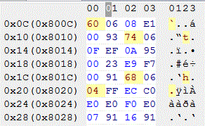
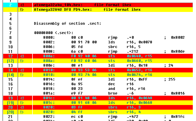
    800a:    f0 92 40 06     sts    0x0640, r15
...
    8010:    00 93 53 06     sts    0x0653, r16
...
    801c:    00 91 48 06     lds    r16, 0x0648
    8020:    03 ff           sbrs    r16, 3
...
    80de:    f0 92 53 06     sts    0x0653, r15

As an exercise, work out which registers are being accessed. The STS and LDS commands are direct store and load instructions. SBRS is “skip if bit in register is set”. In this case we can see bit 3 is being used, which is as it should be, and the value in register 16 is the IN value for the port.

Suppose we want to change the sensing pin to be Port D pin4 (physically pin 24 on a 44 pin xmega). This indicates a base address of 0x0660 and changing the instructions to:

STS  0x0660, R15
...
STS  0x0674, R16
...
LDS  R16, 0x0668
SBRS R16, 4
...
STS  0x0674, R15

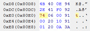
Open Tiny Hexer and import the Intel Hex file appropriate to your chip from the AVR1916 zip file. Now it is just a case of changing the hex representation of the appropriate bytes. Note that the byte order of 0x0640 is reversed in the disassembly and in the HEX file. Here are some screenshots of Tiny Hexer after changing the required bytes:

tinyhexer1

Now export from Tiny Hexer as Intel HEX, saving with a new name (!).

At this point, it is a good idea to run avr-objdump again, on the new HEX file, to make sure that it still makes sense to an AVR. I also did a file-diff on the new vs original disassembled files. The results are as follows, although there is also a block of FF that got inserted between code blocks. This has no effect, and simply reflects the fact that Tiny Hexer exported a continuous block rather than two blocks with a space in between.

Compare PC3 PD4 a

Compare PC3 PD4 b

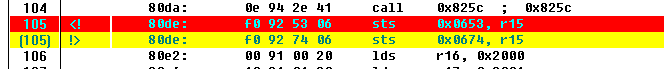
Looks like I got it right! Only the instructions I wanted to change got changed, and the flash memory addresses came out correct for a bootloader.

All that remains is to program this onto the chip with your programmer of choice (I use the Olimex AVR-ISP-MK2 clone since my Dragon utterly fails to even get the device ID 95% of the time), making sure the BOOTRST flag is correctly set if it is a new chip. Erase the chip, program and go!

A Cheat

If you can find two HEX DFU bootloader files for the same target chip, but with different sensing pins, a quick thing to do is to disassemble both and do a diff. I bet they will be from the same basic source code, and will quickly reveal which instructions need changing. Confession: that is how I got started on this problem.

Uploading Using DFU

To be honest, I think FLIP is a bit rubbish, and using the command line batchisp.exe is a pain in the arse. I’ve found dfu-programmer to be much nicer to play with (although the 0.7.1 version does contain a bug that fails to account for the xmega bootloader living in separate flash and so reduces the available flash for applications; this is fixed in 0.7.2 but is not released AFAIK at the time of writing).

I use dfu-programmer from Atmel Studio as an “external tool” via a small “bat file” command script.

In Atmel studio, point the external tool command at the .bat file and add the following into the “arguments” slot:

"$(ProjectDir)Debug\$(ItemFileName).hex" atxmega32a4u

To work, you do need to select the project file with the same name as the hex file before invoking the tool.

My .bat file just contains:

@echo off
REM supply the hex file location as 1st argument e.g. "dfu-programmer script argument blink.hex",
REM supply the target device as the 2nd arg e.g. atxmega32a4u

ECHO Erase, flash %1 and application launch.
ECHO Device = %2
ECHO ==========================================================
ECHO.

SET PATH=%PATH%;C:\Users\Adam\Desktop\dfu-programmer
dfu-programmer %2 erase --force
dfu-programmer %2 flash %1 --debug 2
dfu-programmer %2 launch --no-reset
ECHO -----------------------------------------------------------

Further Adventure?

I have not done this, but see this line:

    800e:    08 e1           ldi    r16, 0x18    ; 24

That is setting the value of register 16, which is immediately stored to PIN3CTRL in the original code. A quick look at the datasheet shows that, as expected, this is setting a pull-up on Port C pin 3. Fancy changing that?

… Or maybe change the SBRS to SBRC ?

AVR Dragon Problem: stopped working, not recognised by USB

OK… so my Dragon just stopped working. Plug it in, the status LED just flashes amber and Windows (XP) does not detect it. Re-install the drivers – no, that isn’t it. (BTW, the instructions in the helpfile that comes with Atmel Studio 6 are wrong). Try another PC or using a motherboard USB socket rather than the hub – no, wrong again. Try a different USB cable – nope.

The answer, it seems is to use a USB hub but to do so with the hub’s separate power adapter. After that, I was able to dispense with the power adapter and the Dragon kept working, even after unplugging/re-connecting.

Wierd! There are a number of suggestions on the web that the Dragon draws a heavy current on startup,  so I guess it got into “a bit of a state.”


AVR Timer1 Dead Time Generator Example (ATtiny85)

The ATtiny 25/45/85 datasheet has an intriguing section about the “dead time generator” that I found a little confusing. A little practical example helped me to understand it. The code and logic analyser trace (made using the same analyser and client mentioned in previous posts) appear below. This is just an example to understand how it works. Real applications seem to be principally brushless DC motor control (pdf).

The setup below uses both A and B compare registers with the same compare value and applies some dead time to the B output so that the effect can be easily seen. I was also tempted to play around with the C compare register which sets the value at which the counter resets. Read the code comments for more…

Timer1 with Dead Time
1
2
3
4
5
6
7
8
9
10
11
12
13
14
15
16
17
18
19
20
21
22
23
24
25
26
27
28
29
30
31
32
33
34
35
36
37
38
39
40
41
//set the top count give whole number percentage duty cycles
const unsigned char top = 99;
//40% duty cycle if top=99
const unsigned char compare = 39;
//prescale CLK/8, 8Mz clock and div8 prescale -> 1MHz tick -> appropx 10kHz output with top=99
const unsigned char prescaleTimer = (1<<CS12);
//prescale CLK/4.
const unsigned char prescaleDead = (1<<DTPS11);// div 8 = (1<<DTPS11) | (1<<DTPS10)
// with CLK/4 prescale and 8MHz clock the dead time is 0.5uS per LSB.
// Dead time is delay to rising edge of signal
const unsigned char deadHigh = 0x0F; //8uS dead time for OCR1B. Max 0x0F
const unsigned char deadLow = 0x08; //4uS dead time for /OCR1B
 
int main(void)
{
	//set data direction for output compare A and B, incl complements
	DDRB = (1<<PB4) | (1<<PB3) | (1<<PB1) | (1<<PB0);
 
	//setup timer1 with PWM. Will be using both A and B compare outputs.
	// both compares will be the same but only B will have dead time applied
	OCR1A = compare;
	OCR1B = compare;
	TCCR1 = (1<<PWM1A) | (1<<COM1A0); //Compare A PWM mode with complement outputs
	GTCCR = (1<<PWM1B) | (1<<COM1B0); //Compare B PWM mode with complement outputs
 
	//PLLCSR is not set so the PLL will not be used (are using system clock directly - "synchonous mode")
	//OCR1C determines the "top" counter value if CTC1 in TCCR1 is set. Otherwise "top" is normal: 0xFF
	OCR1C = top;
	TCCR1 |= (1<<CTC1);
	TCCR1 |= prescaleTimer; 
 
	//setup dead time for compare B. Note the prescaler is independent of timer1 prescaler (both receive the same clk feed)
	DTPS1 = prescaleDead;
	//DT1A is unset - output A has no dead time
	DT1B = (deadHigh<<4) | deadLow;
 
    while(1)
    {
        //do nothing
    }
}
40% duty cycle with no dead time on OC1A and different amounts of dead time added to OC1B and its complement.
Checking the dead time matches what is expected. The fractional differences can be ascribed to a combination of the on-chip clock oscilator not being exactly 8MHz with a minor addition effect from the logic analyser sampling rate (100Mhz)

End Stuff

Source code is also available from github.

All code is copyrighted and licenced as follows:

***Made available using the The MIT License (MIT)***
Copyright (c) 2012, Adam Cooper

Permission is hereby granted, free of charge, to any person obtaining a copy of this software and associated documentation files (the “Software”), to deal in the Software without restriction, including without limitation the rights to use, copy, modify, merge, publish, distribute, sublicense, and/or sell copies of the Software, and to permit persons to whom the Software is furnished to do so, subject to the following conditions:

The above copyright notice and this permission notice shall be included in all copies or substantial portions of the Software.

THE SOFTWARE IS PROVIDED “AS IS”, WITHOUT WARRANTY OF ANY KIND, EXPRESS OR IMPLIED, INCLUDING BUT NOT LIMITED TO THE WARRANTIES OF MERCHANTABILITY, FITNESS FOR A PARTICULAR PURPOSE AND NONINFRINGEMENT. IN NO EVENT SHALL THE AUTHORS OR COPYRIGHT HOLDERS BE LIABLE FOR ANY CLAIM, DAMAGES OR OTHER LIABILITY, WHETHER IN AN ACTION OF CONTRACT, TORT OR OTHERWISE, ARISING FROM, OUT OF OR IN CONNECTION WITH THE SOFTWARE OR THE USE OR OTHER DEALINGS IN THE SOFTWARE.

AVR ADC #2 – Experiments in Operating the ADC at High/Low Sample Rates (ATtiny85)

This article builds on the previous one.

This experiment was stimulated by wanting to have a 128kHz system clock but still be able to use the ADC. Section 17.5 of the datasheet clearly says:

… requires an input clock frequency of between 50kHz and 200kHz to get maximum resolution. If a lower resolution than 10 bits is needed, the input clock frequency to the ADC can be higher than 200 kHz to get a higher sample rate. It is not recommended to use a higher input clock frequency than 1 MHz.

Section 17.8 goes on to say:

The ADC is optimized for analog signals with an output impedance of approximately 10 kΩ or less. If such a source is used, the sampling time will be negligible. If a source with higher impedance is used, the sampling time will depend on how long time the source needs to charge the S/H capacitor, with can vary widely. The user is recommended to only use low impedant sources with slowly varying signals, since this minimizes the required charge transfer to the S/H capacitor.

There is some information on the web, particularly about the limitations of ATtiny/mega for high symbol rate signal processing but I wanted to try for myself and gather some data. The questions are: how does precision vary as both frequency and impedance vary, especially outside the specified range. Given the information in the datasheet, both the comments above and the general description of the sample and hold circuitry, the worst performance should occur for high impedance and high frequency. It turns out this is observed but the story is a little more interesting.

The Circuit and the Code

This uses the same approach as the previous post.

The circuit is minimal and constructed on breadboard. ICSP from an AVR Dragon was fed into a header and left connected. A 100n cap was bridged from pins 4 to 8 over the IC. Three different potentiometers were used: 250k, 47k, 5k. 5V was supplied from the Dragon.

The same code is used with both a 8MHz and a 128kHz main clock – the fuses are set to use the internal oscillators – and the ADC clock frequency changed using the ADC prescaler; after taking an ADC reading, the prescaler is moved to the next higher division factor. See the code below.

Varying the ADC Clock
1
2
3
4
5
6
7
8
9
10
11
12
13
14
15
16
17
18
19
void Degrade_2(){
	unsigned char result[2];
	for(unsigned char prescale=1; prescale<=7; prescale++){
		//clear then re-assert the prescaler
		ADCSRA &= 0xF8;
		ADCSRA |= prescale;
		//start a conversion
		ADCSRA |= (1<<ADSC);
		//wait for end of conversion
		while (ADCSRA & (1<<ADSC));
		result[1] = ADCL;// datasheet says read low first
		result[0] = ADCH;
		sendBytes(result, 2);
	}
 
	//send a comma to separate readings
	unsigned char comma[]=",";
	sendBytes(comma,1);
}

Results 1: Low ADC Clock Frequency

This was a surprise. With a 128kHz main clock, the ADC gets clocked at from 64kHz down to 1kHz. No degradation of precision was observed, no matter which potentiometer was used and no matter what input voltage was selected.

Everything looked normal on the waveform, with the decreasing ADC clock rate clearly showing up as increasing conversion times.

Zoomed-out view of the ADC Clock Changing Experiment.

So it looks like I can just use a slow clock and not worry about the ADC.

Results 2: High ADC Clock Frequency

For a 8MHz system clock the ADC clock will be 4MHz, 2MHz, 1MHz, 500kHz, 250kHz, 125kHz, 62.5kHz according to the prescale value.

A representative range of input voltages were used for each potentiometer using a multimeter which was disconnected before taking ADC readings. The ADC error is calculated assuming the 62.5kHz reading is correct. Three or more readings were taken for each ADC clock rate to confirm stability; no more than 1LSB variation was observed and the median was used. In all cases 10 bit conversion results are considered.

(click for full size)

Although 4MHz looked OK sometimes, it is clearly very messed up! The effect of higher input impedance is clear but even so, we are getting 8 bit precision for most of the input voltage range at 500kHz. Remember the preferred input impedance is around 10k. Just outside the datasheet max freq, at 250kHz the error is down to the least significant bit. So it looks like this device at least is capable of adequate performance a little bit outside both impedance and frequency ranges.

(click for full size)
NB: the plot is slightly distorted since there is no 2V reading.

The second plot shows more clearly the change of error as the potentiometer is swept across its range. The 3V readings seem to be particulary badly affected by the very high frequencies.

(click for full size)

With a 47k potentiometer, which I consider to be compliant with the datasheet impedance requirement, the results look rather impressive. Even at 4MHz there is only a 3LSB error, i.e. we are getting 8 bits of precision (the top 8 bits of the 10 bit results) give or take some quantization error. Although… I am still rather suspicious of 4MHz and I did not explore a wider range of input voltages. At 2MHz, though, this device looks reliably better than 8 bits across most of the input voltage range.

(click for full size)

The final plot shows the case for 3V, which looks like the worst-case, and neatly summarises how far you can push this ATtiny85. The 5k potentiometer is not really significantly better than the 47k except for 4MHz.

End Stuff

Source code is also available from github. A spreadsheet of results and the plots is also there.

All code is copyrighted and licenced as follows:

***Made available using the The MIT License (MIT)***
Copyright (c) 2012, Adam Cooper

Permission is hereby granted, free of charge, to any person obtaining a copy of this software and associated documentation files (the “Software”), to deal in the Software without restriction, including without limitation the rights to use, copy, modify, merge, publish, distribute, sublicense, and/or sell copies of the Software, and to permit persons to whom the Software is furnished to do so, subject to the following conditions:

The above copyright notice and this permission notice shall be included in all copies or substantial portions of the Software.

THE SOFTWARE IS PROVIDED “AS IS”, WITHOUT WARRANTY OF ANY KIND, EXPRESS OR IMPLIED, INCLUDING BUT NOT LIMITED TO THE WARRANTIES OF MERCHANTABILITY, FITNESS FOR A PARTICULAR PURPOSE AND NONINFRINGEMENT. IN NO EVENT SHALL THE AUTHORS OR COPYRIGHT HOLDERS BE LIABLE FOR ANY CLAIM, DAMAGES OR OTHER LIABILITY, WHETHER IN AN ACTION OF CONTRACT, TORT OR OTHERWISE, ARISING FROM, OUT OF OR IN CONNECTION WITH THE SOFTWARE OR THE USE OR OTHER DEALINGS IN THE SOFTWARE.

AVR ADC #1 – Basic Examples (ATtiny85)

As a precursor to investigating the precision of the AVR analogue to digital converter (on an ATtiny85 but assumed to be similar across many AVR devices) outside the recommended ranges of conversion frequency and input impedance, I set about to get to know the ADC better with a couple of “elementary” examples:

  • a simple read in a while(1) loop
  • a read triggered by Timer0

A Preliminary Diversion – observing the process with a logic analyser

There seemed like three main ways to see what the results were:

  1. transmit the results using the serial interface provided on the ATtiny and capture with a logic analyser
  2. as (1) but capturing the bytes on a PC (etc)
  3. direct display using an LCD or LEDs

#1 has the benefit of allowing inspection of the timing as well as capture of results. I have an “Open Logic Sniffer“, which is a great bit of kit for getting to know your MCU and it is a bargain (although has a few minor oddities), which I use with the Logic Sniffer Java Client. The OLS client has some nice analyser features. This was my choice, not least because I had zero experience with the ATtiny Universal Serial Interface (USI).

#2 sounds OK but the USI isn’t quite as universal as it might be – no USART – and I couldn’t be bothered to set up an arduino to relay data, although that is on my “to do” list. Also, I did want to watch the timing.

#3 looked like too much effort on an 8 pin device, given the objective.

Given my zero experience with the USI, I opted for a 3-wire setup that gives a signal that can be understood as SPI; the ATtiny plays the role of a master and just blasts out bytes assuming there is nothing to receive. The OLS client can decode the signals and serve up the transmitted bytes.

 
First we must setup the USI and data direction. Note that “DO” is the data out line but that Atmel have given this the synonym “MISO”, which makes sense if the ATtiny is a slave or is being programmed with an ICSP. PB0 is used as a “slave select” signal, which makes for easier interpretation of the signal traces in OLS, both by humans and the SPI analyser.

Code to setup ATtiny85 for 3-wire mode
1
2
3
4
5
6
7
8
9
10
11
12
13
14
//values to set USICR to strobe out
const unsigned char usi_low = (1<<USIWM0) | (1<<USITC);
const unsigned char usi_high = (1<<USIWM0) | (1<<USITC) | (1<<USICLK);
 
//setup pins for serial
//  PB2 (SCK/USCK/SCL/ADC1/T0/INT0/PCINT2)
// 	PB1 (MISO/DO/AIN1/OC0B/OC1A/PCINT1)
// 	PB0 (MOSI/DI/SDA/AIN0/OC0A/OC1A/AREF/PCINT0) - will not be used as DI
//	PB0 used as /CS
DDRB = (1<<DDB0) | (1<<DDB2) | (1<<DDB1);// /CS, USCK and DO as outputs
PORTB |= (1<<PB0);//slave not selected
 
//setup serial comms - 3 wire
USICR = (1<<USIWM0);

The following is called whenever one or more bytes should be sent out.

Code to send bytes in 3-wire mode
1
2
3
4
5
6
7
8
9
10
11
12
13
14
15
16
17
18
19
20
21
22
23
24
25
26
27
28
29
30
31
32
//sends the specified byte as serial (Three wire style).
void sendBytes(unsigned char bytes[], unsigned char size){
	//slave select
	PORTB &= ~(1<<PB0);
 
	//loop over bytes
	for(unsigned char b = 0; b<size;b++){
		//load the byte to the output register
		USIDR = bytes[b];
		//strobe USICLK 8 cycles (also toggles clock output thanks to USITC)
		//an unrolled loop gives 50% duty and saves 3 clock cycles per bit sent
		USICR = usi_low;
		USICR = usi_high;
		USICR = usi_low;
		USICR = usi_high;
		USICR = usi_low;
		USICR = usi_high;
		USICR = usi_low;
		USICR = usi_high;
		USICR = usi_low;
		USICR = usi_high;
		USICR = usi_low;
		USICR = usi_high;
		USICR = usi_low;
		USICR = usi_high;
		USICR = usi_low;
		USICR = usi_high;		
	}//bytes loop	
 
	//slave de-select
	PORTB |= (1<<PB0);		
}

Testing this with a “Hello World!” message

Say Hello World! in 3-wire mode
		unsigned char send[] = "Hello World!";
		sendBytes(send, sizeof(send)-1);	//-1 drops the null

and running through the OLS Client SPI Analyser tool gives:

(click for full size)

This is “mode 0” SPI style; see that the data is shifted out on a falling SCK and sampled on a rising edge. The alternating high and low assignments to USICR give a USI clock period 1/2 of the main clock since each assignment is a single cycle operation. Both can be seen in the following trace, which shows b01100100 being shifted out.

SCK (serial clock) vs Main Clock Timing and Illustration of Mode 0.

General Structure of the Code and Other Notes

Inside main() I first do some setup then I have a while(1) loop inside which is a function call. Each example/experiment exists as a separate function. Although this leads to the overhead of a few cycles to call the function, this is convenient in the present cases.

I also blew the fuse “CKOUT = [X]” so that the system clock is accessible to the logic analyser.

Simple Example

This assumes the fuse setting “SUT_CKSEL = INTRCOSC_8MHZ_6CK_14CK_0MS”, i.e. an 8MHz internal clock. Make sure that the logic analyser sampling rate is 20MHz or higher otherwise the clock signal will be mis-captured.

perform a single read and send H and L bytes to serial
1
2
3
4
5
6
7
8
9
10
11
12
13
14
15
16
//assumes 8MHz clock, hence prescaling 
void SimpleRead(){
	//set prescaler to div64 --> 125kHz ADC clock
	ADCSRA |= (1<<ADPS2) | (1<<ADPS1);
	//start a conversion
	ADCSRA |= (1<<ADSC);
	//wait for end of conversion
	while (ADCSRA & (1<<ADSC))
	{
		//do nothing
	}
	unsigned char result[2];
	result[1] = ADCL;// datasheet says read low first
	result[0] = ADCH;
	sendBytes(result, 2);
}
SPI Analysis Results from OLS Client

Since this waits until the ADC conversion has finished, the interval between readings is effectively controlled by the time it takes for conversion. This is, in turn, determined by the ADC clock. The datasheet indicates the ADC clock should operate at between 50kHz and 200kHz. The datasheet also says a conversion takes 13 ADC clock cycles. Given the prescaling (code above), the conversion should take 13*64 = 832 cycles. The logic analyser (no screenshot shown) shows 901 cycles between /CS rising (happens at the end of sendBytes just before returning) and /CS falling again (happens just after entering sendBytes on the subsequent reading). Hence there are 69 main clock cyles spent doing other things: returning from sendBytes, returning from SimpleRead, process the while(1), call SimpleRead, setting ADCSRA, processing the while loop in SimpleRead, retrieving the low and high bytes, calling sendBytes. There is clearly some waste here that should be avoided in many real applications.

Timer-triggered Example

This is a rather more interesting example in which Timer0 is configured to trigger ADC conversion when the timer value = the “compare A” value. During both the timer delay and the ADC conversion, software is free to do other things since timer and ADC are hardware-controlled. At the end of the conversion an interrupt is triggered to do something with the result. In this case, just to send it out to serial.

Note that this example uses the 128kHz “watchdog” clock (fuse: “SUT_CKSEL = WDOSC_128KHZ_6CK_14CK_0MS”) to give a long enough timer 0 interval for me to detect the delay. I also used a 2s delay to change the ADC input during execution and make sure it is being properly captured. This means I had to reduce the ISP clock for in-system programming; I used 16kHz, which is reliable if slow.

The code is as follows, noting that Init_TimerTriggered() need only be called once. Note also the last line in the interrupt service routine… that one took me a while to work out!

Timer Triggered ADC
1
2
3
4
5
6
7
8
9
10
11
12
13
14
15
16
17
18
19
20
21
22
23
24
25
26
27
28
29
30
//setup for TimerTriggered
void Init_TimerTriggered(){
	//1. enable ADC completion interrupt
	sei();//global interrupts
	ADCSRA |= (1<<ADIE);//ADC interrupt
 
	//2. set the ADC to be timer triggered
	ADCSRB |= (1<<ADTS1) | (1<<ADTS0); //this defines the trigger source
	ADCSRA |= (1<<ADATE);//this is needed to enable auto-triggering
 
	//3. setup timer
	TCNT0 = 0x00;//counter to 0
	TCCR0A =  (1<<WGM01);//use "clear timer on compare match" mode
	OCR0A = 0x80;//output compare to 128 gives about 1s with 128kHz sys clock and prescaler (below)
	TCCR0B = (1<<CS02) | (1<<CS00);//prescaler to 1024, which enables the counter
}
 
//ADC completion interrupt service.
//Sends the data from the ADC register
ISR(ADC_vect)
{
	//read and send ADC
	unsigned char result[2];
	result[1] = ADCL;// datasheet says read low first
	result[0] = ADCH;
	sendBytes(result, 2);
 
	//clear timer compare flag otherwise the ADC will not be re-triggered!
	TIFR |= (1<<OCF0A);
}

Given the slower clock, the logic analyser sample rate and total capture package can be reduced too. I used a capture trigger (type=complex mode=serial in OLS… read the OLS tutorial!) to watch for /CS falling so 1kB of capture data at 500kHz sampling is ample to capture one timer-driven event.

The captured trace (following ADC completion), just for completeness is:

End Stuff

Source code is also available from github.

All code is copyrighted and licenced as follows:

***Made available using the The MIT License (MIT)***
Copyright (c) 2012, Adam Cooper

Permission is hereby granted, free of charge, to any person obtaining a copy of this software and associated documentation files (the “Software”), to deal in the Software without restriction, including without limitation the rights to use, copy, modify, merge, publish, distribute, sublicense, and/or sell copies of the Software, and to permit persons to whom the Software is furnished to do so, subject to the following conditions:

The above copyright notice and this permission notice shall be included in all copies or substantial portions of the Software.

THE SOFTWARE IS PROVIDED “AS IS”, WITHOUT WARRANTY OF ANY KIND, EXPRESS OR IMPLIED, INCLUDING BUT NOT LIMITED TO THE WARRANTIES OF MERCHANTABILITY, FITNESS FOR A PARTICULAR PURPOSE AND NONINFRINGEMENT. IN NO EVENT SHALL THE AUTHORS OR COPYRIGHT HOLDERS BE LIABLE FOR ANY CLAIM, DAMAGES OR OTHER LIABILITY, WHETHER IN AN ACTION OF CONTRACT, TORT OR OTHERWISE, ARISING FROM, OUT OF OR IN CONNECTION WITH THE SOFTWARE OR THE USE OR OTHER DEALINGS IN THE SOFTWARE.