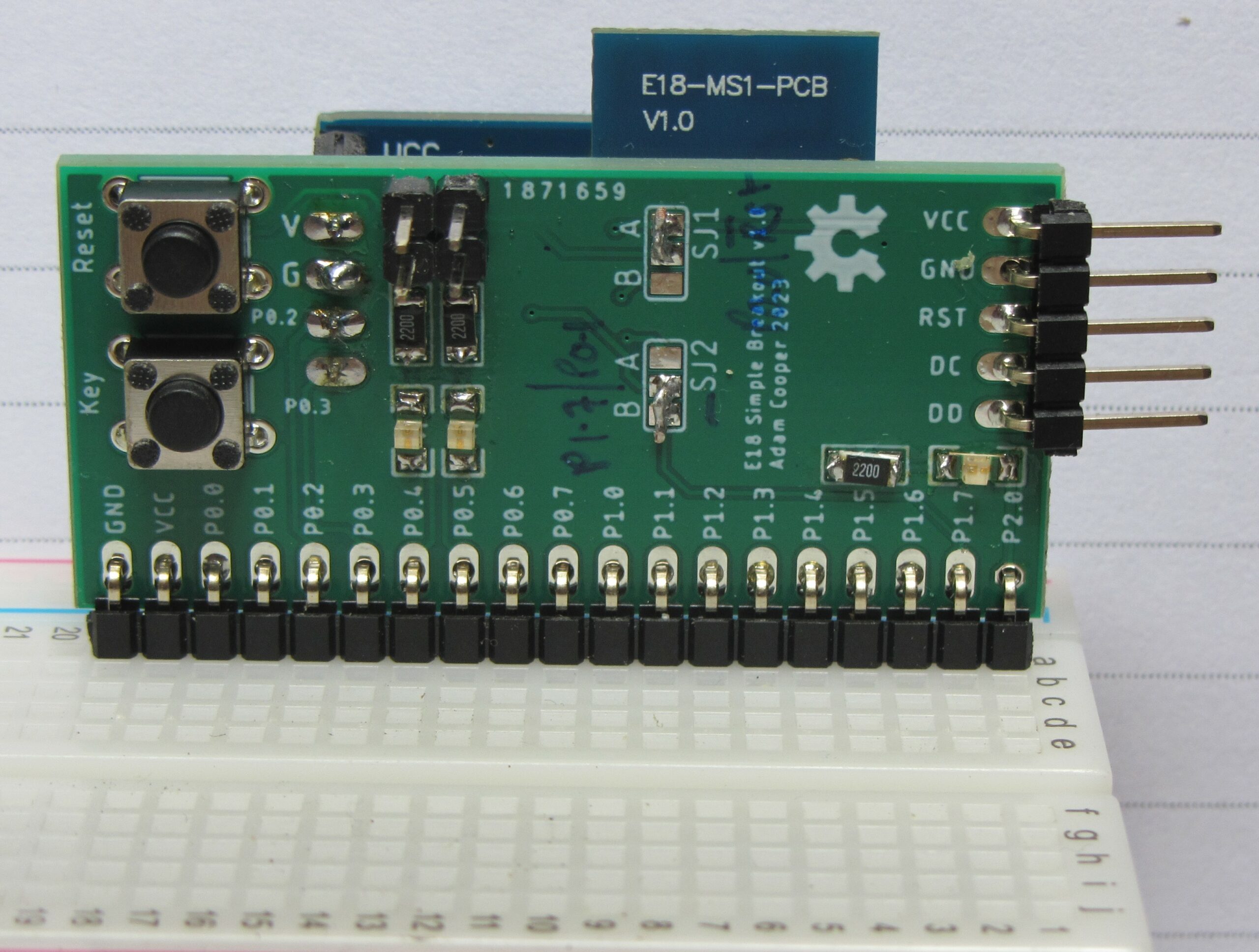
Having recently wanted to get my hands dirty with DIY Zigbee – see my other post on low cost DIY Zigbee – I couldn’t find any suitable breakout boards so, after having found the CC2530-based Ebyte E18-MS1 modules (which are rather economical and available from the manufacturer on Aliexpress… and seemingly without the curse of a glut of clones and fakes), I decided to make my own.
I wanted something quite simple but also flexible, with maximal scope for experimenting and learning. The main use case is to plug into breadboard but there was enough PCB space for some “convenience” components: two switches and three LEDs and associated resistors.
This is what it looked like once assembled (you can just see a BH1750 I2C light sensor on the rear):
Some notes on motivation, layout pragmatics, and options:
The long header is meant to be populated with right-angle pins. This will put the antenna nicely up and leaves plenty of space for other components on the breadboard (I find the breakouts with very wide dual-in-line pin-outs to be rather irritating, and Arduino style sockets and flying leads are not great when more than a few connections are to be made).
The 5 pin header is for firmware flashing. I opted for this, rather than the full 10 pin “debug” header which CCDebugger uses, for econonmy of space. These 5 pins are quite sufficient for using CCDebugger with TI SmartRF Flash Programmer (I made a little adapter) or if using something like Flash CC2531, which works fine for CC2530’s, (or my patched version for use with Pi v1 GPIOs).
The 4 pin header may be convenient for either UART or I2C connections. I’m expecting to be using PTVO and for the CC2530 it fixes UART pins to be P0.2 and P0.3. This header is meant to be mounted on the same side as the E18 module (opposite to switches).
The switches should be configured using the solder jumpers.
SJ1 handles the “Reset” button: A connects to E18 Reset; B connects to P0.0.
SJ2 handles the “Key” button: A connects to P0.1; B connects to P1.7 (which is used by the E18 factory firmware).
The on-board LEDs (and the enabling jumpers) visually correlate with the pins they are connected to: P0.4, P0.5, and P2.0.
Eagle does not lend itself to unusual, possibly artistic, board outlines copper tracks, silk screen etc. There are a number of Eagle ULPs (user language programs) that can import DXF files, and yet more which import bit maps as a mass of polygons, but I struggled to get any of them to work, or simply balked at the number of fiddly steps required. Basically: it was just too hard or error-prone. Then I stumbled across an article by Shabaz Yousaf complaining about the same problem but pointing to HPGL (Hewlett Packard Graphics Language) as a solution. He provides a C program to do the conversion but: a) I wanted to make a ULP for ease of use and b) I wanted to add some configurability at run-time. This article outlines the approach I took. I am assuming that images are created from the outset in Inkscape but Inkscape can import many formats, so it should be possible to use it on existing images, and any graphics software supporting HPGL output should work (HPGL appears to be very simple, but it may be the case that other software creates HPGL in a way my code does not recognise… so your mileage may vary!).
The User Language Program – hpgl2scr
The latest version is in my GitHub ULP repository (direct link to ULP). Please report bugs via GitHub if possible. Also any friendly guidance; this is my first ULP. This is available under an open source licence.
It should be fairly self-explanatory to use after a bit of messing about. Note that the wire (or polygon boundary) width auto-changes depending on the layer that is chosen. Adding more layers is easy by editing the ULP.
Some notes on usage:
HPGL files can contain several separate lines (think a pen moving about in an old-school plotter). Hpgl2scr creates one or more paths of wires or polygon boundaries in the specified layer.
A .scr file is created in the same folder as the .hpgl input. This file may be used to repeat the import.
In normal use choose the Wire output type. When using polygon output, note that setting the pour type = cutout may be used after import for subtractive effects (but only for copper layers).
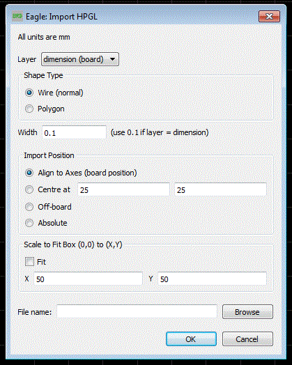
All units are mm.
The imported image can be positioned in four ways:
Aligned to the x and y axes with all wires at positive coordinate values, i.e. in the correct position for a board outline.
Centred at a chosen position.
Off-board (on the opposite side of the origin compared to option 1). This is the best place to group-select the shape and manually move it into place.
Absolute positioning; (0,0) of the original graphic maps to (0,0) on the board. Absolute positioning may be useful if several layers are used in an image and each converted to separate HPGL files for separate importing. Beware that the origin for Inkscape is top left, whereas for boards in Eagle it is bottom left.
The Scale to Fit Box setting will rescale the image (preserving aspect ratio) so that it fits within a box of the specified size (in mm). This is quite useful in that it allows Inkscape to be used without worrying about absolute size, but the final board can be within the limits for PCB cost etc.
Using Copper Layers
As imported, copper layers do not form part of the circuit as far as Eagle is concerned. You cannot just connect to them and use them as pre-routed tracks (OK, so you can leave partially-routed tracks but dangling airwires just feels so untidy, and I always check for unrouted airwires so this would just be another cause of missed mistakes). The solution to this problem is to set the name of the imported wire to be the same name as an existing net. Use the “Name” tool to find the name of the airwire you are interested in, and the Name tool again to change the name of the imported wire to match it. Once done, an airwire should appear from your imported wire. The you can now manually route a trace to the imported wire and it connects nicely.
Note: if you now do a “rip-up all”, your imported wire gets ripped up!
Hints and Tips for Inkscape
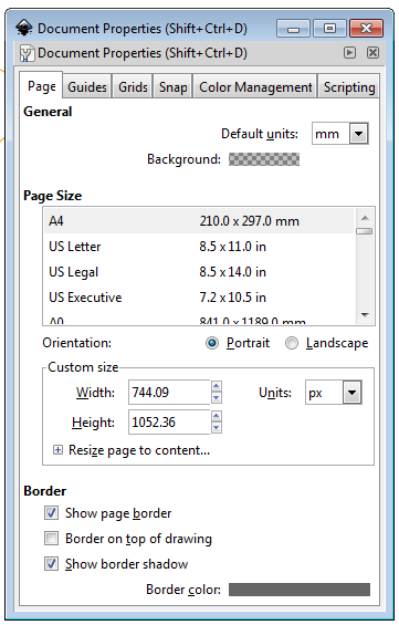
I recommend setting document properties to give mm as the default units (File > Document Properties).
Note that the inkscape image elements MUST be saved as paths (vectors) to export to HPGL. Use the Path menu: Path > Object to Path. If your image does not appear in inkscape check this first!
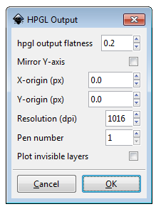
Simply “save as”, selecting the HP Graphics Language file type.
Pen number and flatness are irrelevant. Other parameters should be as shown. Make sure resolution is 1016 dpi if the absolute size matters.
The thickness of the lines in inkscape is irrelevant; the HPGL just follows the path.
Being Ambitious
If you want to be ambitious and to compose several different elements (board outline, various bits of copper and silk) in a single inkscape image you will end up using layers in inkscape. Use a separate inkscape layer whenever the HPGL import parameters will differ (e.g. Eagle layer, wire vs polygon, wire thickness). Make all inkscape layers but one be invisible and export to HPGL, ensuring that the “Plot invisible layers” checkbox is not checked (see the “HPGL Output” screenshot above).
The import will probably be best done with the “absolute” positioning. It would be possible to import “off-board” and to move the elements into place, but positioning will not be easy to replicate in eagle. The trickiness arises because Inkscape uses the top left as origin (0,0), whereas Eagle uses the bottom left. This is easily fixed by checking the “Mirror Y-axis” option on export. Make sure that the image is right down in the bottom left corner so that ends up in roughly the right place in Eagle.
An Example
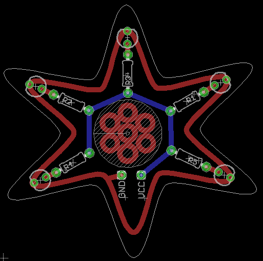
Here is a quickly executed (and slightly wonky) LED star for a “magic wand”. This followed the approach mentioned above of using 2 layers in inkscape. The inner and outer stars were positioned and sized using typed-in values in inkscape and imported one layer at a time with absolute positioning. The imported copper wire was re-named to GND (I had already named the net in the schematic).
It look about 20 minutes, including some time forgetting most of the hints I’ve given!
The problem of panelising PCBs created using the free version of Eagle and gerbmerge is described in an instructible but I found a couple of issues when creating gerbers for Seeed Studio. This outlines the issues and my approach in brief; it is mostly a public note to myself to remember what to do next time. The account that follows assumes the guidance in the instructible is followed by default.
The issues stem from use of the “.BOR” and “.GML” gerber layers. Seeed’s instructions do not mention BOR files and they do say that the board outline should be in a GML file, which is supposed to be the milling control. My guess is that if you do not send a GML file, Seeed will use whatever is in the silk layer to guess the board outline. My board had some milled slots for a power connector.
Step 1 – make sure the CAM file emits the right Eagle layers to the right Gerbers
Start the CAM processor and open the CAM file provided by Seeed. It would be silly not to!
Click the “Add” button to create a new job section. Change Job|Section to (e.g.) Board Outline and change the output device to GERBER_RS274X. Style should have only “pos.coord” and “Optimize” ticked. Change the file name to %N.BOR
Select layer Nr 20 (Dimension).
That defines the .BOR file that gerbmerge needs to lay out the panel.
Next, select the “Slot drills/holes” tab. Note the file is %N.GML. Layers 20 and 46 should be selected. De-select layer 20.
Note that this should probably not be used for creating gerbers for a board that will not be panelised because the GML file does not contain the board outline as Seeed request.
Step 2 – edit the panel.cfg file for Gerbmerge
Note the existing lines “BoardOutline=%(prefix)s.bor”, one for the merged output and one for each sub-board. These stay as they are.
If there is any milling (check by looking at the GML in a gerber viewer, if you don’t already know), add “*Milling=%(prefix)s.GML” on a separate line in each of the sections where “BoardOutline=%(prefix)s.bor” appears.
Make sure the line “OutlineLayerFile = %(mergeout)s.OLN” does not begin with a “#” character.
Step 3 – panelise and hack
Run gerbmerge as normal.
Note that if there is no milling, is should work fine to rename the merged output OLN file as GML.
Otherwise… a bit of cut and paste hackery is needed to get the final merged board outline and the in-board milling into the GML file. Copy the section from just below the line with only a % character to the end of the OLN file and paste this into the merged GML file just below the same point, making sure that the last line from the OLN does not get merged with an existing line in the GML.
Now check all the panelised gerber files in a viewer!
This information is provided without warranty; if your boards come back wrong its your fault, not mine.