This article builds on the previous one.
This experiment was stimulated by wanting to have a 128kHz system clock but still be able to use the ADC. Section 17.5 of the datasheet clearly says:
… requires an input clock frequency of between 50kHz and 200kHz to get maximum resolution. If a lower resolution than 10 bits is needed, the input clock frequency to the ADC can be higher than 200 kHz to get a higher sample rate. It is not recommended to use a higher input clock frequency than 1 MHz.
Section 17.8 goes on to say:
The ADC is optimized for analog signals with an output impedance of approximately 10 kΩ or less. If such a source is used, the sampling time will be negligible. If a source with higher impedance is used, the sampling time will depend on how long time the source needs to charge the S/H capacitor, with can vary widely. The user is recommended to only use low impedant sources with slowly varying signals, since this minimizes the required charge transfer to the S/H capacitor.
There is some information on the web, particularly about the limitations of ATtiny/mega for high symbol rate signal processing but I wanted to try for myself and gather some data. The questions are: how does precision vary as both frequency and impedance vary, especially outside the specified range. Given the information in the datasheet, both the comments above and the general description of the sample and hold circuitry, the worst performance should occur for high impedance and high frequency. It turns out this is observed but the story is a little more interesting.
The Circuit and the Code
This uses the same approach as the previous post.
The circuit is minimal and constructed on breadboard. ICSP from an AVR Dragon was fed into a header and left connected. A 100n cap was bridged from pins 4 to 8 over the IC. Three different potentiometers were used: 250k, 47k, 5k. 5V was supplied from the Dragon.
The same code is used with both a 8MHz and a 128kHz main clock – the fuses are set to use the internal oscillators – and the ADC clock frequency changed using the ADC prescaler; after taking an ADC reading, the prescaler is moved to the next higher division factor. See the code below.
1 2 3 4 5 6 7 8 9 10 11 12 13 14 15 16 17 18 19 | void Degrade_2(){ unsigned char result[2]; for(unsigned char prescale=1; prescale<=7; prescale++){ //clear then re-assert the prescaler ADCSRA &= 0xF8; ADCSRA |= prescale; //start a conversion ADCSRA |= (1<<ADSC); //wait for end of conversion while (ADCSRA & (1<<ADSC)); result[1] = ADCL;// datasheet says read low first result[0] = ADCH; sendBytes(result, 2); } //send a comma to separate readings unsigned char comma[]=","; sendBytes(comma,1); } |
Results 1: Low ADC Clock Frequency
This was a surprise. With a 128kHz main clock, the ADC gets clocked at from 64kHz down to 1kHz. No degradation of precision was observed, no matter which potentiometer was used and no matter what input voltage was selected.
Everything looked normal on the waveform, with the decreasing ADC clock rate clearly showing up as increasing conversion times.

So it looks like I can just use a slow clock and not worry about the ADC.
Results 2: High ADC Clock Frequency
For a 8MHz system clock the ADC clock will be 4MHz, 2MHz, 1MHz, 500kHz, 250kHz, 125kHz, 62.5kHz according to the prescale value.
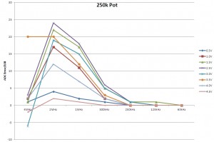
A representative range of input voltages were used for each potentiometer using a multimeter which was disconnected before taking ADC readings. The ADC error is calculated assuming the 62.5kHz reading is correct. Three or more readings were taken for each ADC clock rate to confirm stability; no more than 1LSB variation was observed and the median was used. In all cases 10 bit conversion results are considered.

Although 4MHz looked OK sometimes, it is clearly very messed up! The effect of higher input impedance is clear but even so, we are getting 8 bit precision for most of the input voltage range at 500kHz. Remember the preferred input impedance is around 10k. Just outside the datasheet max freq, at 250kHz the error is down to the least significant bit. So it looks like this device at least is capable of adequate performance a little bit outside both impedance and frequency ranges.

NB: the plot is slightly distorted since there is no 2V reading.
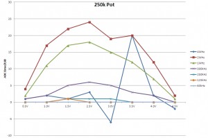
The second plot shows more clearly the change of error as the potentiometer is swept across its range. The 3V readings seem to be particulary badly affected by the very high frequencies.

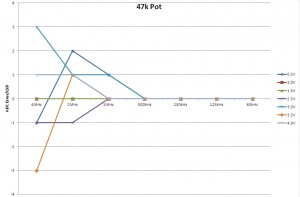
With a 47k potentiometer, which I consider to be compliant with the datasheet impedance requirement, the results look rather impressive. Even at 4MHz there is only a 3LSB error, i.e. we are getting 8 bits of precision (the top 8 bits of the 10 bit results) give or take some quantization error. Although… I am still rather suspicious of 4MHz and I did not explore a wider range of input voltages. At 2MHz, though, this device looks reliably better than 8 bits across most of the input voltage range.

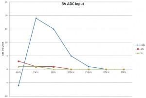
The final plot shows the case for 3V, which looks like the worst-case, and neatly summarises how far you can push this ATtiny85. The 5k potentiometer is not really significantly better than the 47k except for 4MHz.
End Stuff
Source code is also available from github. A spreadsheet of results and the plots is also there.
All code is copyrighted and licenced as follows:
***Made available using the The MIT License (MIT)***
Copyright (c) 2012, Adam CooperPermission is hereby granted, free of charge, to any person obtaining a copy of this software and associated documentation files (the “Software”), to deal in the Software without restriction, including without limitation the rights to use, copy, modify, merge, publish, distribute, sublicense, and/or sell copies of the Software, and to permit persons to whom the Software is furnished to do so, subject to the following conditions:
The above copyright notice and this permission notice shall be included in all copies or substantial portions of the Software.
THE SOFTWARE IS PROVIDED “AS IS”, WITHOUT WARRANTY OF ANY KIND, EXPRESS OR IMPLIED, INCLUDING BUT NOT LIMITED TO THE WARRANTIES OF MERCHANTABILITY, FITNESS FOR A PARTICULAR PURPOSE AND NONINFRINGEMENT. IN NO EVENT SHALL THE AUTHORS OR COPYRIGHT HOLDERS BE LIABLE FOR ANY CLAIM, DAMAGES OR OTHER LIABILITY, WHETHER IN AN ACTION OF CONTRACT, TORT OR OTHERWISE, ARISING FROM, OUT OF OR IN CONNECTION WITH THE SOFTWARE OR THE USE OR OTHER DEALINGS IN THE SOFTWARE.
Very interesting post. we *can* push the ADC clock a bit faster then!
If I understand the circuit correctly, the pot impedance will be max around mid wiper or 2.5V, and near 0 ohms around 0V and 5V. This would explain the 250k pot plot, in which the greatest ADC errors are around the mid range pot settings.
Just a note on this quote:
“Even at 4MHz there is only a 3LSB error, i.e. we are getting 8 bits of precision (the top 8 bits of the 10 bit results)”
Actually, LSB with regard to ADC error already has an accepted meaning in the industry. LSB is normally used as a unit corresponding to the magnitude of one step, rather than the x lowest bits.
But nevertheless, useful post for a project I have in the pipeline. Something else you kight want to try, putting a 100n or so decoupling cap on the ADC and see if it reduces the error. (Assuming the error might be related to sudden current spikes during the conversion.)
Hi –
thanks for the correction and suggestion.
Adam